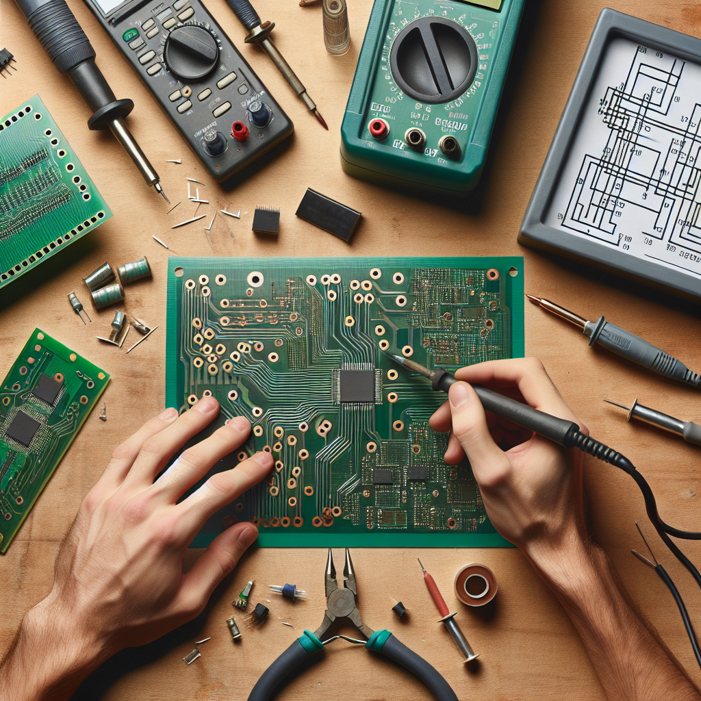
How to Create Printed Circuit Boards?
Printed Circuit Boards (PCBs) are essential components in almost all electronic gadgets. They provide the physical and electrical connections required to enable the functioning of electrical circuits. Learning how to create your own PCB can be a fulfilling and educational endeavor. This article will guide you through the step-by-step process of creating printed circuit boards, from designing to manufacturing, while detailing necessary tools and techniques required.
Understanding the Basics of Printed Circuit Boards
Before diving into the creation process, it’s essential to understand the basics of a PCB. A printed circuit board is made up of a thin layer of conducting material, such as copper, which is laminated onto a non-conductive substrate. Components are then soldered onto this conductive layer, forming an electrical circuit. Here are the basic materials and tools you will need:
Materials and Tools Needed
| Material/Tool | Description |
|---|---|
| Copper-Clad Board | A board with a thin layer of copper on one or both sides |
| Etching Solution | A chemical solution to remove unwanted copper |
| Soldering Iron | A tool to solder components onto the board |
| Drill | For making holes in the PCB |
| PCB Design Software | Used to design the layout of the circuit |
| UV Light Box | For transferring the design onto the board (if using photosensitive boards) |
| Protective Gear | Gloves, goggles, etc., for safety |
Steps to Create a PCB
1. Designing the Circuit
The first step in creating a PCB is to design the circuit using PCB design software. This software allows you to layout your circuit diagram, place components, and create the necessary electrical connections. Popular PCB design software includes Eagle, KiCad, and Altium Designer.
Steps for Designing the Circuit
- Open your PCB design software
- Draw the schematic diagram
- Design the PCB layout
- Place components
- Route the traces
- Verify the design with a Design Rule Check (DRC)
2. Printing the Design
Once the design is complete, the next step is to print it onto a transparent sheet for transferring it to the copper-clad board. If you’re using a laser printer, print your design onto a glossy or photo paper. Ensure that the design is printed in a mirror image.
3. Transferring the Design to the Copper Board
To transfer the printed design to the copper board, place the printed layout face down on the copper surface. Using a hot iron or a UV light box, transfer the pattern onto the copper board. The heat or UV light will transfer the ink onto the copper-clad board, creating a masked area that will protect the copper below it.
4. Etching the Board
Submerge the masked copper board into an etching solution, typically made of ferric chloride or ammonium persulfate. The solution will dissolve the unmasked copper, leaving only the copper traces that are protected by the transferred pattern.
5. Drilling Holes
After etching, wash the board thoroughly to remove any remaining etching solution. Next, drill holes where components will be mounted. Use a precision drill to make small, accurate holes as specified in your design.
6. Soldering Components
With the holes drilled, start placing and soldering the electronic components onto the board. Use a steady hand and a suitable soldering iron for this step. Make sure each component is correctly placed and soldered as per the design specification.
7. Testing the Board
Once all components are in place, it’s crucial to test the board for any short circuits or incorrect connections. Use a multimeter to check continuity and ensure there are no shorts. Power up the board carefully and test its functionality according to your design requirements.
Common Mistakes to Avoid
While creating PCBs, you might encounter several common mistakes. Here are some tips to avoid them:
- Incorrect Component Placement: Double-check your design and placement before soldering.
- Poor Soldering Technique: Practice and ensure you have the right soldering equipment.
- Design Errors: Always perform a Design Rule Check (DRC) in your software.
- Incomplete Etching: Monitor the etching process closely and ensure all unwanted copper is removed.
Conclusion
Creating your own printed circuit boards can be an enriching experience, providing you with a deeper understanding of electronics and circuit design. By following these steps closely and avoiding common mistakes, you can successfully create functional and reliable PCBs. Always remember to prioritize safety by using proper protective gear and handling chemicals with care.


Leave a Comment