
Panduan Paling Sederhana untuk Mengakses Modem Motorola Anda
Memiliki kontrol penuh atas modem Motorola Anda adalah hal yang penting. Ini tidak hanya membantu dalam mengelola koneksi internet, tetapi juga memberi Anda kemampuan untuk memodifikasi pengaturan jaringan, memantau aktivitas, dan memperbaiki masalah teknis. Panduan ini akan memberikan langkah-langkah mengakses modem Motorola dengan cara yang paling sederhana.
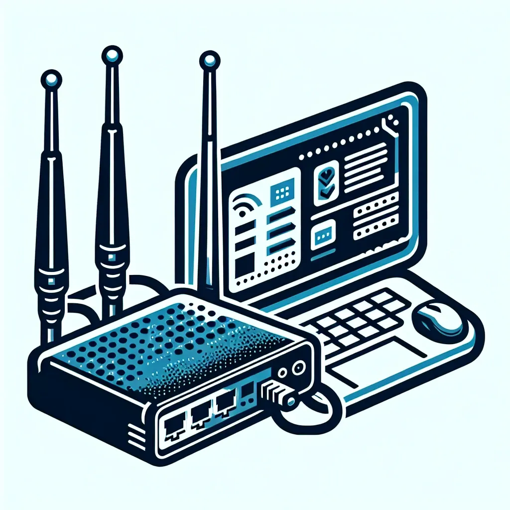
Langkah-langkah Mengakses Modem Motorola
Berikut adalah langkah-langkah untuk mengakses modem Motorola Anda:
- Menghubungkan Komputer ke Modem: Pastikan bahwa komputer atau perangkat Anda terhubung ke modem Motorola menggunakan kabel Ethernet atau melalui koneksi Wi-Fi.
- Membuka Browser Web: Gunakan browser web pilihan Anda seperti Google Chrome, Mozilla Firefox, atau Microsoft Edge.
- Memasukkan Alamat IP Modem: Ketik alamat IP modem Motorola Anda ke bilah alamat browser. Biasanya alamat ini adalah http://192.168.0.1 atau http://192.168.100.1.
- Masukkan Username dan Password: Pada halaman login, masukkan username dan password Anda. Username dan password bawaan biasanya adalah ‘admin’ untuk keduanya, kecuali Anda telah mengubahnya sebelumnya.
Alamat IP Umum untuk Modem Motorola
| Model Modem | Alamat IP Default |
|---|---|
| Motorola SB6121 | 192.168.100.1 |
| Motorola MB7420 | 192.168.0.1 |
| Motorola MG7550 | 192.168.0.1 |
Fitur-Fitur Utama pada Modem Motorola
- Halaman Status: Memberikan informasi tentang koneksi internet, kecepatan koneksi, dan status perangkat jaringan.
- Pengaturan Jaringan: Mengizinkan Anda untuk mengubah pengaturan LAN, DHCP, DNS, dan lainnya.
- Keamanan: Menawarkan pengaturan firewall dan fitur keamanan lainnya untuk melindungi jaringan Anda dari ancaman.
- Firmware Update: Memungkinkan Anda untuk memperbarui firmware modem untuk meningkatkan kinerja dan keamanan.
Pemecahan Masalah Umum
Masalah Username dan Password
Jika Anda lupa username atau password, reset modem ke pengaturan pabrik dengan menekan tombol reset selama 10 detik. Proses ini akan mengembalikan semua pengaturan ke default.
Koneksi Internet Terputus
Periksa kabel fisik dan pastikan semua koneksi tersambung dengan benar. Restart modem dan router sesuai kebutuhan.
Lambatnya Kecepatan Internet
Pastikan tidak ada aplikasi yang menggunakan bandwidth secara berlebihan. Juga cek dengan ISP Anda untuk memastikan tidak ada masalah jaringan dari sisi mereka.
Kesimpulan
Modem Motorola menyediakan sejumlah opsi yang cukup lengkap untuk mengelola jaringan Anda. Dengan mengakses halaman administrasi modem Anda, Anda dapat dengan mudah mengontrol dan mengoptimalkan kinerja jaringan Anda. Panduan sederhana ini dimaksudkan untuk membantu Anda dalam memahami dan mengakses modem Motorola Anda dengan cara yang mudah dan efisien.


Leave a Comment